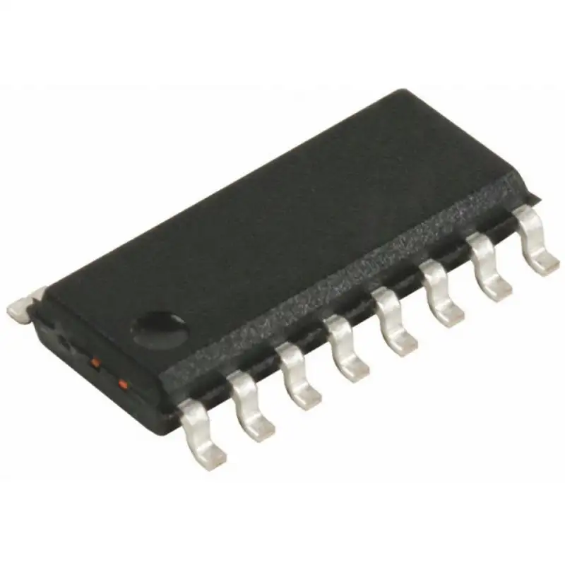
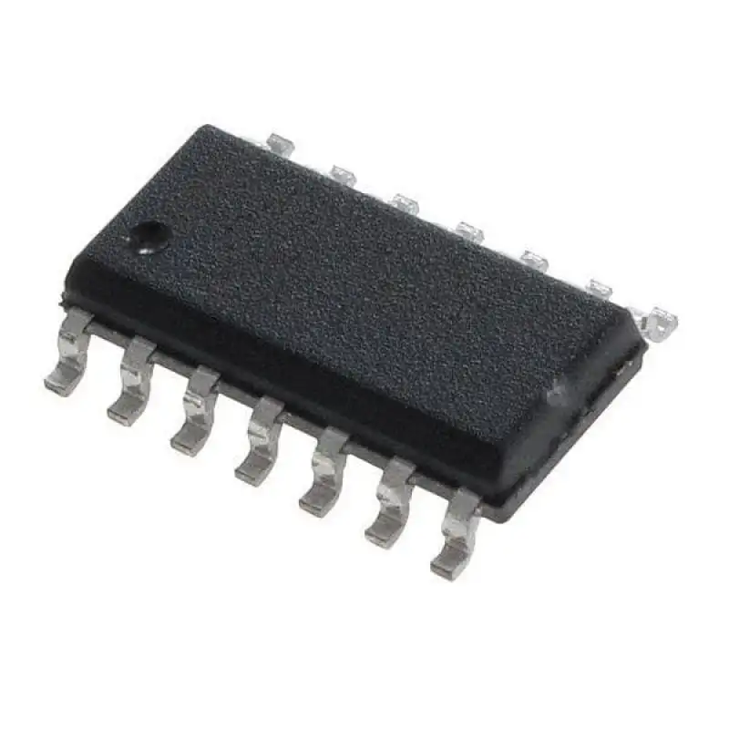
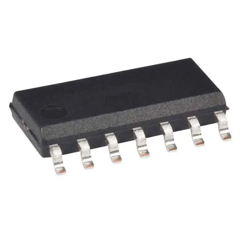
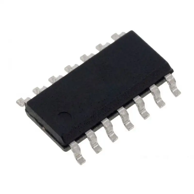
CD4052 IC - (SMD Package) - Differential 4-channel Multiplexer/Demultiplexer IC
$36.86
$53.07
The CD4052 analog multiplexers/demultiplexers are digitally controlled analog switches having low “ON†impedance and very low “OFF†leakage currents. Control of analog signals up to 15Vp-p can be achieved by digital signal amplitudes of 3−15V. For example, if VDD = 5V, VSS = 0V and VEE = −5V, analog signals from −5V to 5V can be controlled by digital inputs of 0−5V. The multiplexer circuits dissipate extremely low quiescent power over the full VDD−VSS and VDD−VEE supply voltage ranges, independent of the logic state of the control signals. When a logical “1†is present at the inhibit input terminal all channels are “OFFâ€. A, B, and C, and an inhibit input. The three binary signals select 1 of 8 channels to be turned “ON†and connect the input to the output. CD4052 is a differential 4-channel multiplexer having two binary control inputs, A and B, and an inhibit input. Features:- • Wide range of digital and analog signal levels: digital 3 – 15V, analog to 15Vp-p • Low “ON†resistance: 80Ω (typ.) over entire 15Vp-p signal-input range for VDD − VEE = 15V • High “OFF†resistance: channel leakage of ±10 pA (typ.) at VDD − VEE = 10V • Logic level conversion for digital addressing signals of 3 – 15V (VDD − VSS = 3 – 15V) to switch analog signals to 15 Vp-p (VDD − VEE = 15V) • Matched switch characteristics: ∆RON = 5Ω (typ.) for VDD − VEE = 15V • Very low quiescent power dissipation under all digital-control input and supply conditions: 1 µ W (typ.) at VDD − VSS = VDD − VEE = 10V • Binary address decoding on chip Specification:- Symbol Parameter Values VDD DC Supply Voltage −0.5 VDC to 18 VDC VIN Input Voltage 0.5 VDC to VDD 0.5 VDC TS Storage Temperature −65°C to 150°C PD Power Dissipation 700 mW TL Lead Temperature 260°C Related Document:- CD4052 SMD Data Sheet